Over the last few weekends I have been spending some time in learning how to make your own PCBs at home. While there are many online service vendors who do an excellent job for a reasonably good price for bulk quantity, I felt they are a bit of an over kill for single order PCBs – particularly for my project – where the circuits are pretty straight-forward. For single PCBs, I determined making them myself. Plus this gives me an opportunity to learn this skill without spending too much money.
Tools of the Trade:
- Press-n-Peel Blue (I bought mine here)
- Access to a computer
- Laser Printer (not dot-matrix or ink jet)
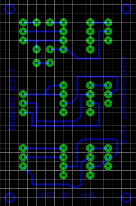
- A board drawing software. I use “Eagle“
- Paper cutter (with a good sharp blade)
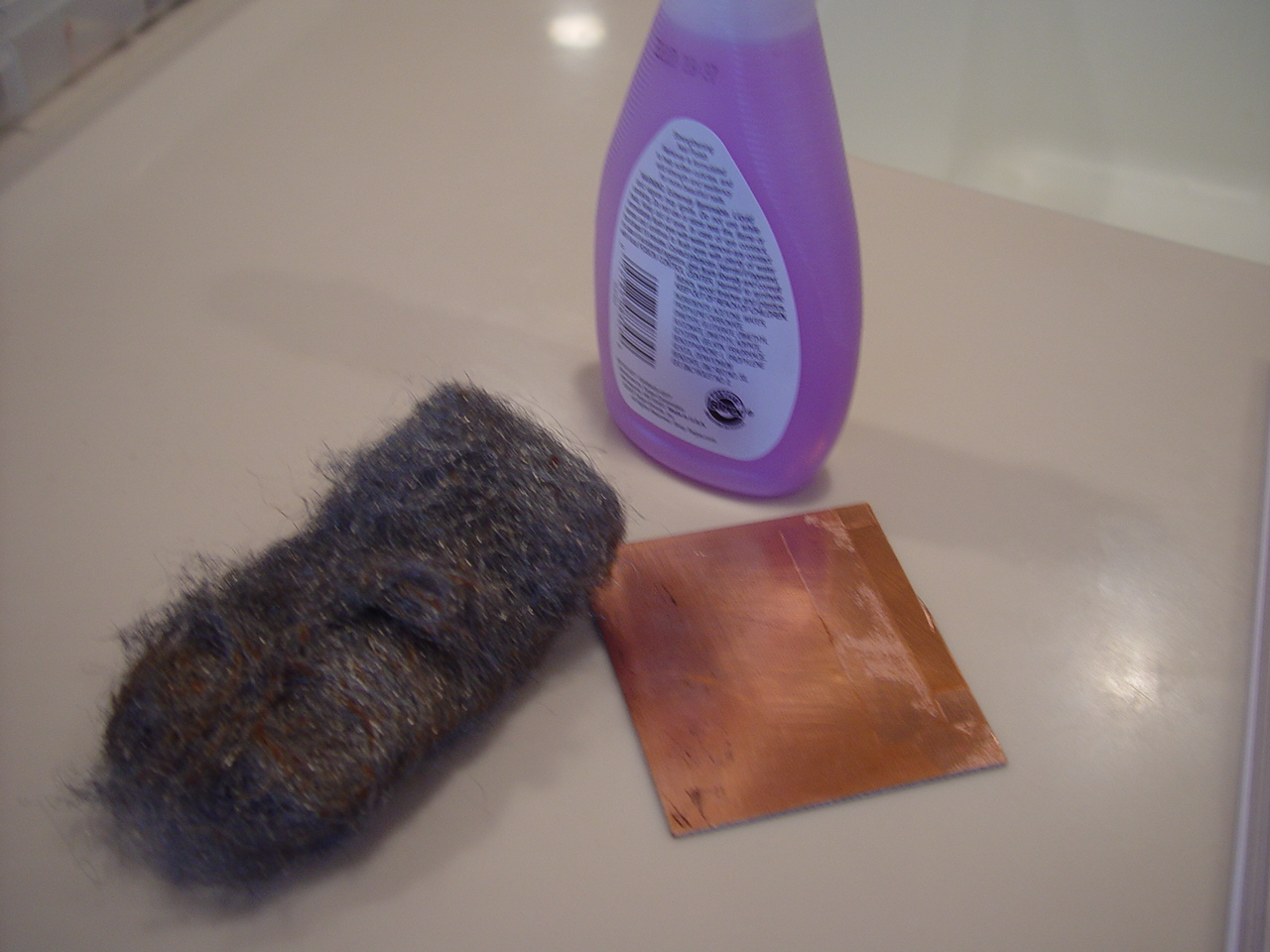
- PCB board panel
- Ferric Chloride Soln (I bought mine here)
- Masking Tape
- Pressing Iron
- Number 70 Drill bit (I bought mine here)
- A hand-press drilling tool or a drill machine w/ drill press
- a plastic tray
- Steel wool
- Some Alcohol for washing the PCB (my wife would know – I stole her nail-polish-cleaner-thingy)
Steps:
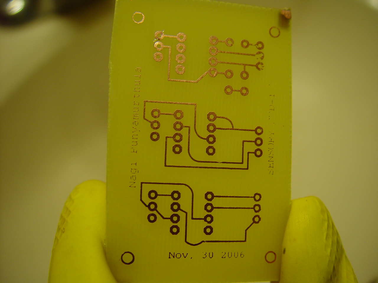
Circuit Transfer to PCB:
- Design your board and print it out on paper using a laser printer
- Before printing,
- ensure that the “Solid” option is selected on your Eagle software
- Also ensure, you pick 300 dpi vs 600 dpi. The 300 dpi ensures the pins alignment is accurate

- Before printing,
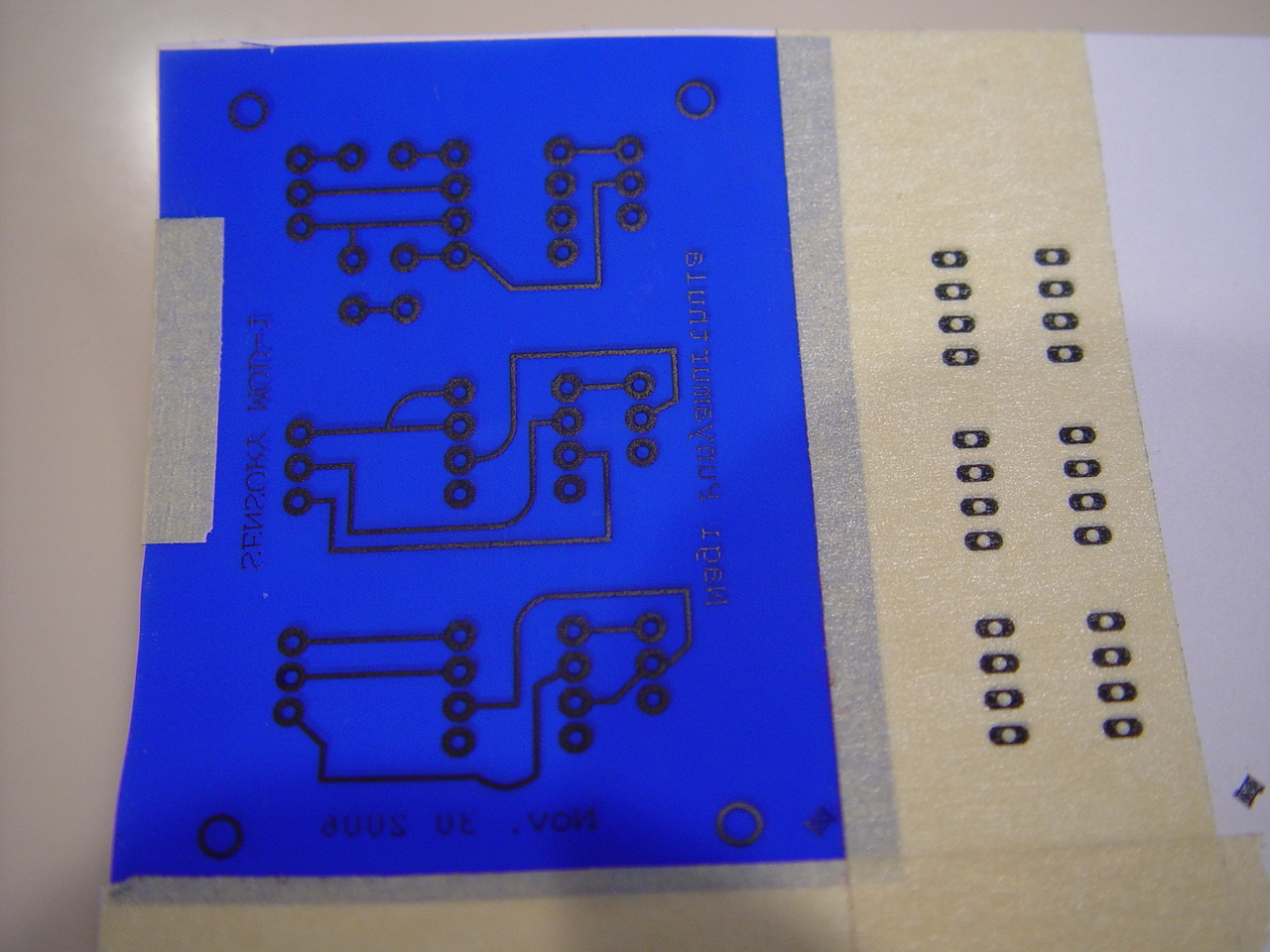
- Take your Press-N-Peel paper and cut to fit the printed board drawing – add about 1/2″ extra on all sides
- Use a paper cutter to get the square edges on the P-n-P paper.


- With the DULL side of P-n-P cut paper facing UPWARDS, tape it over the printer paper (using thin masking tape) w/ the printed drawing so that the P-n-P covers the drawing on the printer paper.
- Make sure you line up the P-n-P paper with the edges.


- Now, place the P-n-P that is over the printed paper facing DOWN into the printer tray (check w/ your printer specs, yours might need it facing up). I’m using HP Laser 6P – which needs it facing down.
- Now RE-PRINT the drawing from Eagle software
- By now, the Drawing is now printed on the DULL side of the P-n-P paper
- While the drawing is being printed, set up your press-iron to either “wool” or “polyester” setting. Let it heat up. Temperature is very CRITICAL
- Carefully remove the P-n-P paper from the printer paper making sure your DON’T touch the dull side w/ your fingers. Finger prints can cause issues later on
- Carefully remove the masking tape from printer paper and the P-n-P
- Carefully set aside the P-n-P in a dust free place. Use a small plastic box to cover over it.

- Now, take the PCB copper panel and using steel wool and some alcohol wipe and wash off the panel.


- make sure you don’t touch the face of the panel board
- Repeat the washing 2-3 times to make sure the face is bright and shiny and void of any goo spots
- Now, using a clean paper towel, wipe of the PCB panel so that it is completely dry and free of any felt or other remains.
- Starting now on, ensure you touch and lift the PCB board ONLY by its corners
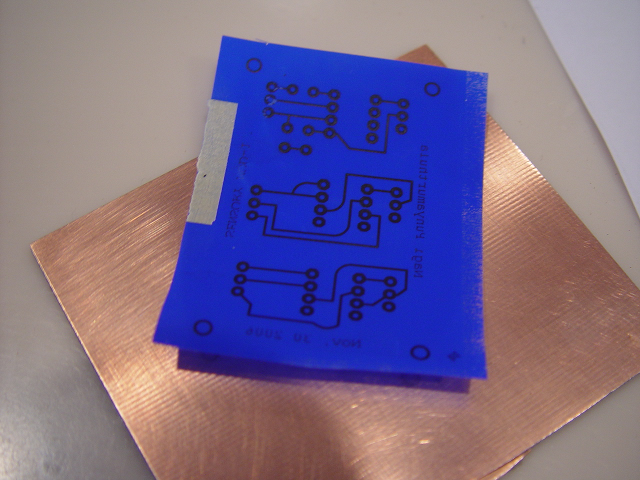
- Once the PCB is all dry
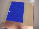
- take the prepared P-n-P w/ the drawing
- with the DULL side facing DOWN, line it up over the cleaner face of the PCB panel.
- And, using thin masking tape, tape the edges – making sure your are NOT covering up the drawing.
- Make sure there are no ripples or air bubbles – we want full contact over the PCB


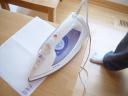
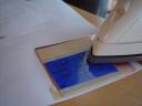
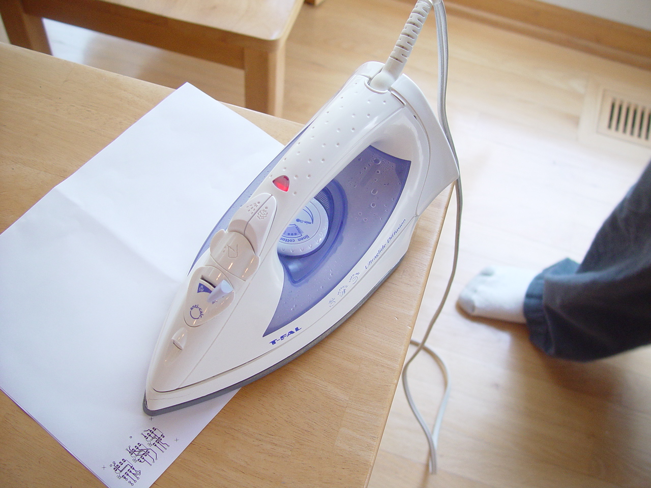
- While this moment, your pressing-iron must be ready by now.
- On a flat surface, lay a paper down (printer paper should work well)
- SWITCH OFF the steam setting on your iron – NO STEAM
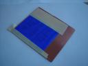
- With the P-n-P side facing UP, place the PCB over the paper (step 12.2)
- Now take another paper and lay it OVER the PCB
- Take your iron and place it over the PCB and press firmly over moving it about over the PCB.
- We need to ensure the heat is transfered to the PCB evenly
- After abt 3 minutes of firm presses and moving the iron about over the PCB, set the iron over the PCB and leave it alone for about 4 minutes
- Now, again, with firm presses move about the iron for another 3 minutes making sure you are running the iron right over the P-n-P side of the PCB
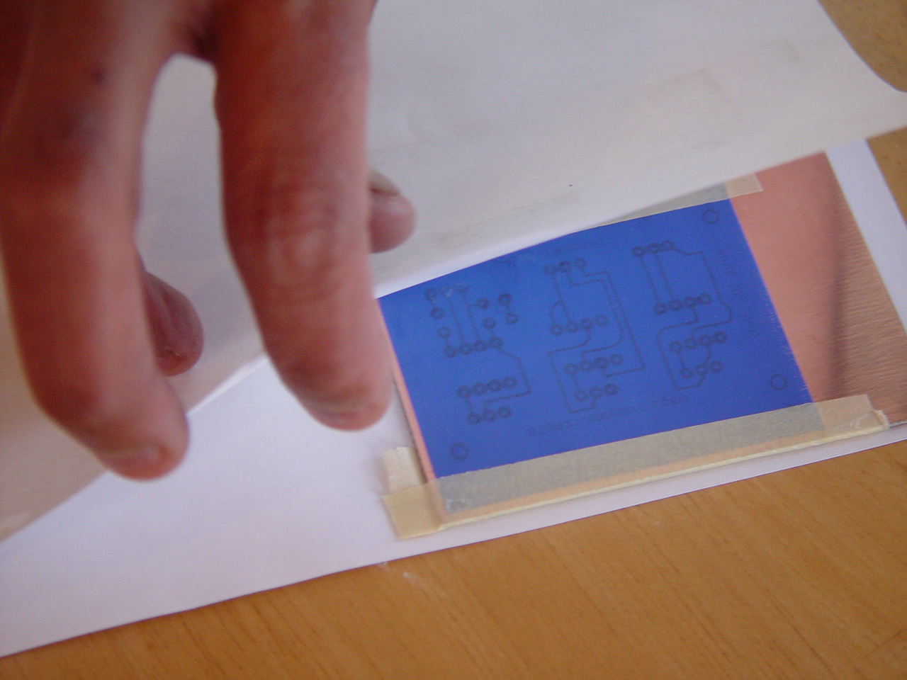
- Now take away the printer paper that was place over the PCB
- Using your iron, move about the iron with firm presses over the P-n-P DIRECTLY (w/o the paper over it), making sure you’re catching all the corners


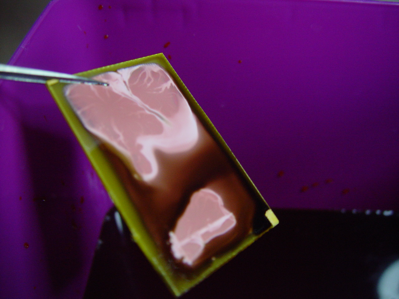
- At this time, you can check the status of the transfer of the drawing over to the PCB by briefly lifting the P-n-P from the PCB.
- Once all the drawing is transfered to the PC, you can safely remove the P-n-P completely from the PCB
- You’re now done w/ transfering the drawing to the PCB
- Switch off the iron
- Carefully peel off and separate the P-n-P from the PCB.
- Make sure again, you are NOT touching the PCB face


- Let the PCB cool off for 2 minutes – be careful PCB will be HOT
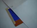
- Take the PCB and cut to size using the paper cutter- It worked great for me. Making sure you are NOT cutting off the drawing – that would be bad and defeats the purpose.

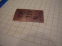


Etching:
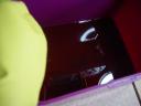
- In a plastic container – prefereably w/ a deep flat one
- Place the PCB, with the drawing facing up
- WARNING:
- Pour the Ferric Chloride just enough to cover the PCB
- Now using both your hands, tilt the plastic container to/fro and side-to-side alternating
- do this for about 10 minutes
- At this time, the copper coating over the PCB should start eroding and eventually should be gone
- Leaving alone the drawing portion of the PCB


- Once the drawing side is free of all copper, using your tweazers, turn the PCB bottom side up
- Now again using both your hands, tilt the plastic container to/fro and side-to-side alternating
- do this for about 10 minutes
- At this time, the copper coating over this side of PCB should start eroding and eventually should be gone


- Now again using both your hands, tilt the plastic container to/fro and side-to-side alternating
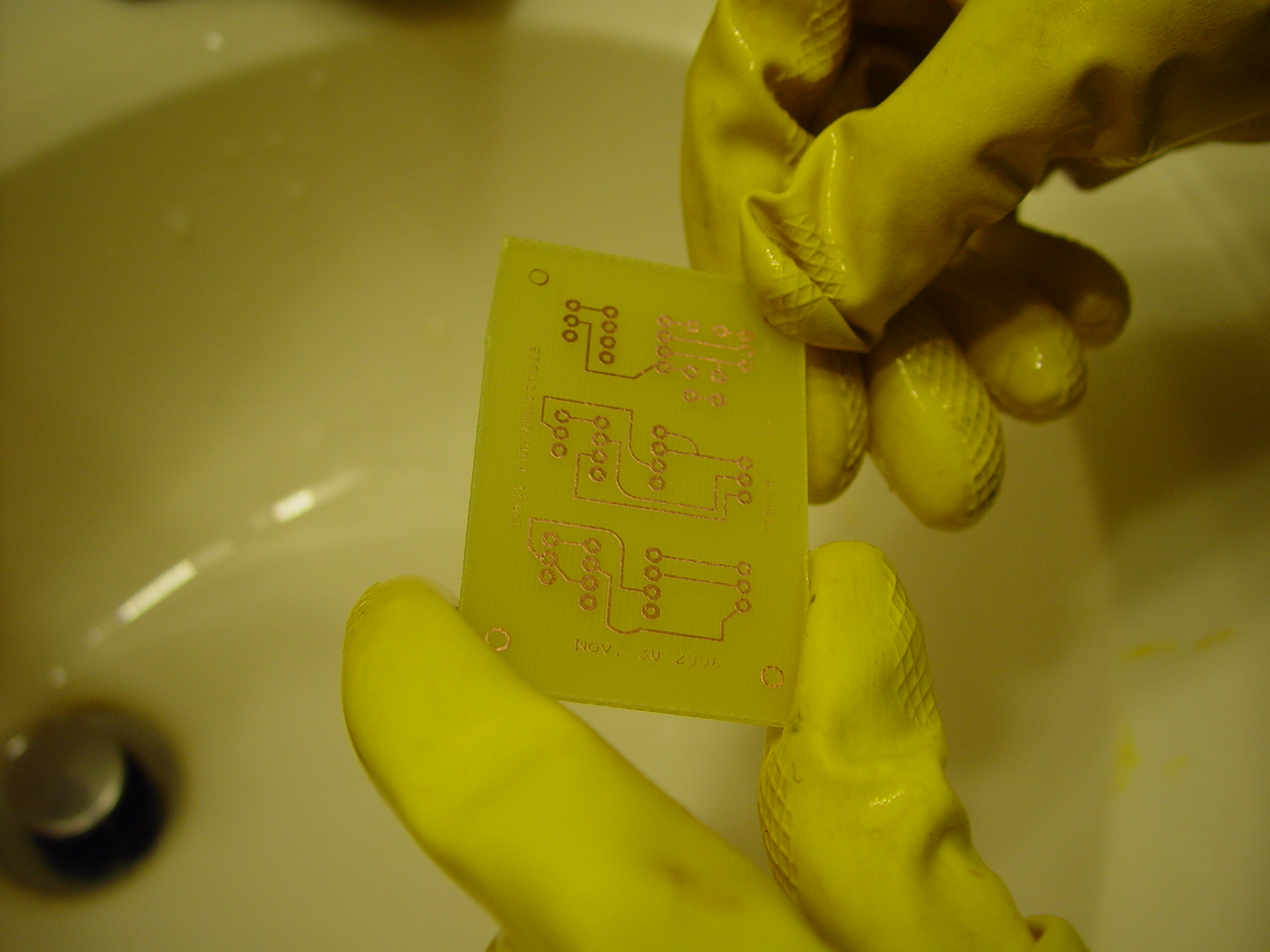
- Once all the copper is gone over all the parts of the PCB except the drawing portion, carefully take out the PCB to a sink with running tap water.
- Place the PCB under running water making sure the PCB is completely washed free of any left over chemical


- Now with steel wool, firmly rub over the drawing areas of the PCB while letting it run under the running tap.
- Wipe off with dry cloth or paper towel
- Discard the chemical under running tap water – you don’t want any stains left


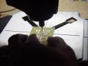
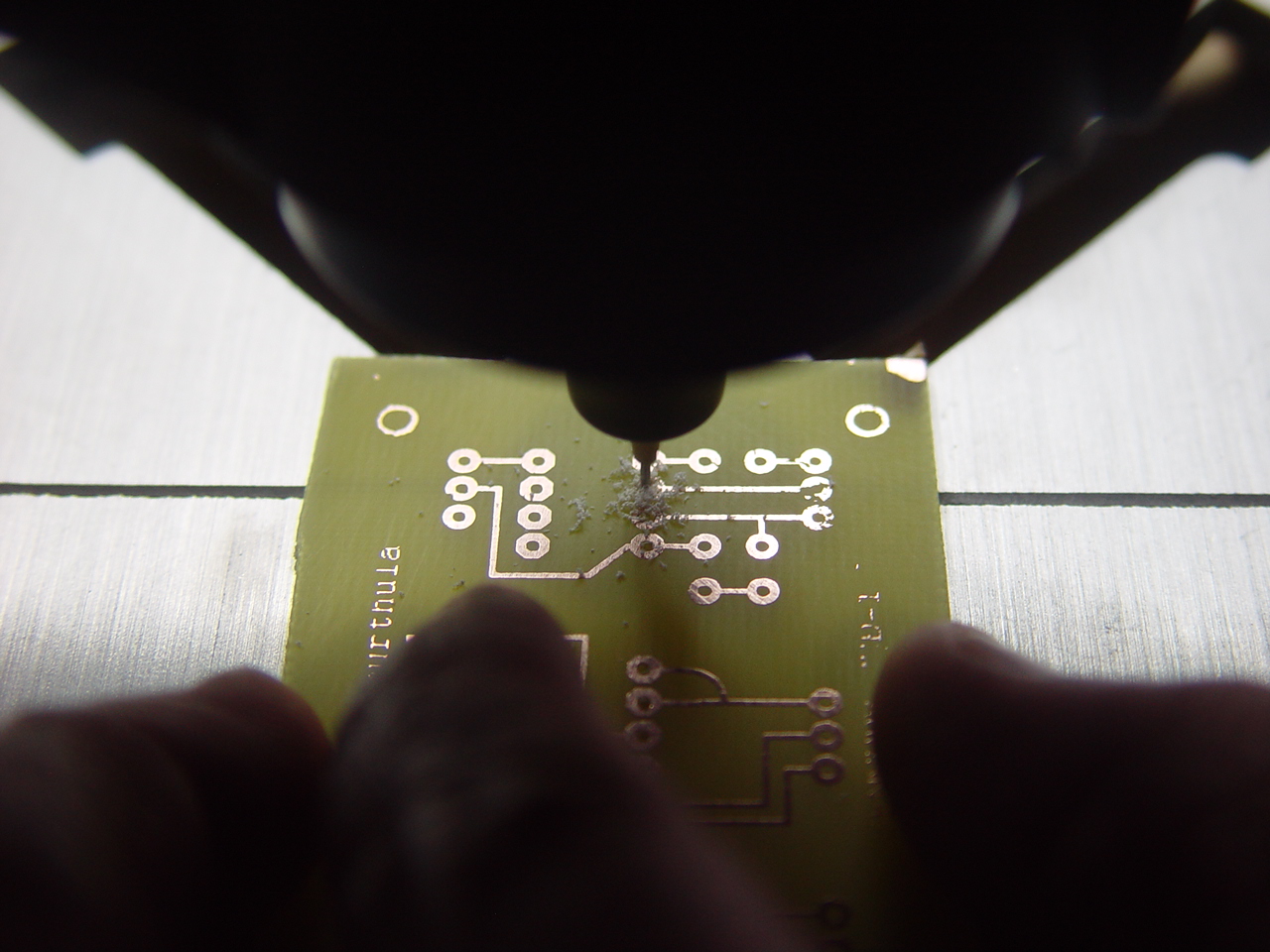
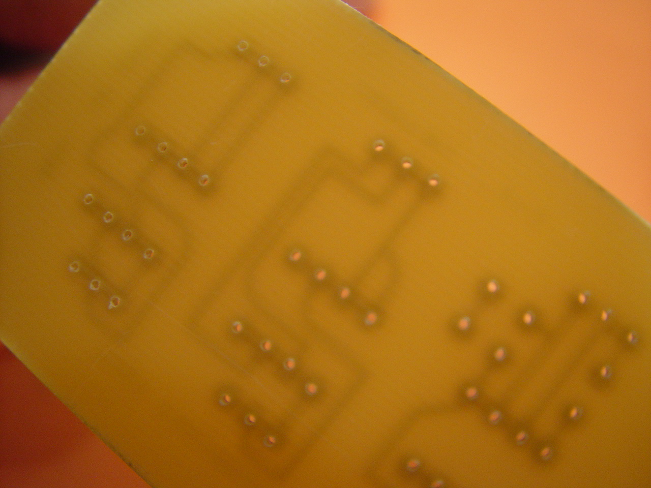
Drilling:
- For drilling holes thru the vias, I am using a #70 drill bit and a Dremel drill housed over a workbench
- line up each of the PCB hole targets and vias and start drilling away.


You’re now a successful PCB Homebrewer!
This was my 2nd attempt to making my own PCBs and this board took me 35 minutes start-finish.
Hope that was useful and helpful in your experiments
BTW, thanks to my dear wife for taking these pictures. Had to sneak that in there!!
ciao
Nagi

January 25, 2007 at 10:50 pm |
How do you make the vias anyway?
January 26, 2007 at 1:03 am |
Hey Nagi! nice tutorial!!!…
but i need to tell you some things…. firs you dont need to cover all the PCB.. you can use less chemical and put the copper face looking down (the pcb will float in the ferric clhoride)
second do you really want all that chemical (wich eats lots of types of metal)???? you can put it again in the bottle and use it again… also you can heat the chemical before using it and it will act quickly
and also you can replace that kind of paper with a really shiny paper (i dont know the english word for that kind of paper) its kinda photopaper but its not. Well its cheaper and you have to do the same steps
cheers!!!
January 26, 2007 at 2:55 am |
Thanks! Great tutorial for newbie’s like myself.
January 26, 2007 at 3:10 am |
Thank you for this great tutorial! There are some nice technic, I really like the printer solution, were you tape you press-n-peel to the paper and then print it. I saw that your pcb was missing some toner on the pads of one of your chip, you could take a permanent pen and retouch it before ecthing it! Went I made mine, I fill all the holes pads with a pen just in case they could of vanish in the acid. My friend reuse the etching solution. He ecth a board, then he reuse the same acid for a other day(one day you will need to throw it away). If you take your entire plastic container and dips it in a other container with HOT water! This help to etch faster! Some people say that you should not discard of Ferric Sulfate in the sink or toilet… It could cause problems and might even eat throught your pipes!
January 26, 2007 at 3:52 am |
Great tutorial, I have one problem though. I wouldn’t pour the ferric chloride into your sink, it’s sole purpose is to eat metal… pouring it in metal drains seems like a bad idea.
Thanks for the info on blue paper though, thats the only step I was missing XD
January 26, 2007 at 12:58 pm |
Great HOWTO! (got here from hackaday)
Just a question though: aren’t there regional rules for the disposal of etchant? In France, I believe, it needs to be neutralized before disposal in the common sewer system.
If confirmed, it could be nice to add a mention 🙂
January 26, 2007 at 4:50 pm |
[…] Syndicated via RSS from del.icio.us/tag/diy AP World News is on […]
January 26, 2007 at 5:20 pm |
Very nice writeup! This is almost exactly the same method I use.
A couple minor suggestions I would make:
1) scotch-brite pads are also great for cleaning the board instead of steel wool. It may be preferable, because steel wool can leave steel dust embedded in the copper if you don’t clean it perfectly, which can later rust. Not sure if it’s a real problem in practice, but something I’ve heard mentioned and have always avoided steel wool for this reason.
2) It’s often a good idea to carefully trim the press-n-peel very close to the edges of the pattern after printing – the 1/2″ or so margin you leave will sometimes wrinkle and warp under the heat and can cause poorer transfer around the edges. It’s less of a problem when you are using wider traces and pads around the edges.
January 26, 2007 at 8:53 pm |
awesome!
January 27, 2007 at 5:40 pm |
Yeah, huh, no problem with sending all those chemicals down the sink?
February 1, 2007 at 12:14 am |
Instead of using this fancy blue paper-thing you can as well use shiny paper from colorful magazines. Just choose the page with letters only (on the area where your pcb will be printed). Procedure is the same, except that it is good to warm-up the pcb and then stick the printout eventually ironing everything together. When it’s cool just put it in the water and when the paper is wet carefully peel it off. Then use soft kitchen scrubber and vinegar (soft acid) to get rid of the rest of the paper. Do it carefully and the result is perfect. And with NO cost.
February 3, 2007 at 9:37 pm |
Just a side note if you’re using ferric chloride and flushing it down your pipes, what do you think it’s doing to your copper piping? The same thing it’s doing to the exposed copper PCB!!
February 5, 2007 at 10:39 pm |
John,
I agree w/ you. There could be regional regulatory clauses to disposing off the etchant.
For the records 🙂
“Readers, please check w/ your regional govt offices on the disposal regulations of the etchant solns”
thanks John
caio
February 6, 2007 at 6:57 pm |
[…] this has been around but we’ve been thinking about making some homebrew PCBs, so… This DIY is pretty good since it has lots of cool pictures… nice […]
March 17, 2007 at 2:03 am |
copper pipe is only used for incoming water to your home. Not sewer or waste water, at least if your home is in the USA and up to code…
anyway. im having issues with trying to transfer the print from the PNP blue to the PCB. i have my iron cranked up all the way. when i use my infrared temperature thingy on the pcb (actually on the paper between the iron and the PCB) its reading ~350F which is what the directions that came with the PNP paper say. But when i look at the PCB there is no black toner on it. just faded outlines of the traces. Is this whats expected to happen or am i doing something wrong?
March 19, 2007 at 12:33 pm |
chupa,
That temperature seems a bit high – not telling by the temp reading ~350, but, because you’re saying that the ironbox is crancked up all the way high. In my case, I had it soemwhere in the cotton +1 setting.
when printing to the PNP blue, make sure you’re printing to the dull side of the paper and not to the glossy side. After that is done, ensure the dull side is faced down on the PCB and taped on all edges. And, then transfer.
Another point to note is, ensure that the “steam” is OFF on the ironbox.
hope that helps – good luck!
caio
October 17, 2007 at 3:34 pm |
Nagi – I happened upon this while researching how to set up using PnP blue for etching copper in making jewelry components. Very good tutorial, thanks, since the process is the same as what I would be doing. My burning issue at this point is how to get the image on the transfer… Folks say use a photocopier but no place I’ve asked (local Office Max, local library, etc.) will let me put the Pnp through their machines, despite anything I say to reassure them. I am, therefore, thinking of buying a laser printer (my current printer is an inkjet, plus I have a archival quality image printer for art and photo work, but it uses ink so no go there). You say you are using an HP Laser 6P. Is that the same as the HP Laserjet 6P? I’ve located a refurbished one of those for not much money and am considering it. I need to get a recommend for a printer that I know will take the PnP. And that definitely uses a carbon based toner. You would be amazed at how hard it is to get these questions answered by calling manufacturers customer service lines. So… HP Laser 6P = HP Laserjet 6P? Abd you are having no issues with printer jams? Hope you will reply, either her or use my direct email
October 17, 2007 at 3:58 pm |
Robin
yes, it is a HP LaserJet 6P and I have had no problems w/ it.
hope that helps
Nagi